Atom by Atom Manufacturing
Making atomically perfect materials and machines
John N. Randall
President
Zyvex Labs
About the Lecture
Technological progress is limited by manufacturing precision, a relationship first studied by Norio Taniguichi in the 1970s. Revolutionary inventions, even when made into working prototypes, have languished without realizing societal or economic benefits for long periods (hundreds of years) after their invention because manufacturing precision necessary to mass produce them was not available. A contemporary example of precision’s limitation on technology is embodied in Moore’s Law. The fundamental limitation on the growth of integrated circuit capacity is the precision with which circuit features can be reliably manufactured. Taniguichi, who coined the term “nanotechnology,” wondered if there is a fundamental limit on precision. Richard Feynman suggested the possibilities of atomic precision – “there’s plenty of room at the bottom,” he said, and asked what might become possible if we could place atoms one by one exactly where we want them. Several decades later Eric Drexler explored the question in detail and concluded – a lot! Although there have been dramatic demonstrations of such technology Eigler’s “IBM” spelled out in metal atoms on an atomically smooth surface – very few scientists are pursuing atomic precision. The common view is that we don’t need atomically precise structures, at least not beyond molecules. But manufacturing processes that take advantage of the quantization of matter not only should improve manufacturing precision, they promise to achieve absolute precision. Such processes should be able to make things that are not just very close to identical but that in fact are identical. This will be possible when our fabrication processes are digital; that is when we have processes that either will or won’t add an atom or molecule to a specific bonding site. Digital fabrication will replace analog fabrication for the same reasons that digital electronics have replaced analog electronics. But the atomically perfect matter made with these processes – digital matter – will be even more revolutionary. It will be dimensionally perfect and have desirable properties that far exceed anything that can be made today. This talk will describe efforts to develop a digital fabrication process, the difficulties and successes we have achieved, and what we believe will be possible in the not too distant future.
About the Speaker

JOHN RANDALL is President of Zyvex Labs, where he works on nanofabrication technologies and was instrumental in developing and spinning out successful nanotechnology companies Zyvex Technologies and Zyvex Instruments. He also is an Adjunct Professor at UT-Dallas and serves on the External Engineering Advisory Board of the University. Before joining Zyvex, John was with Texas Instruments where he worked in high resolution processing for integrated circuits, MEMS, and quantum effect devices. While at TI, John and the teams he worked with fabricated the first quantum dot diode, developed the first quantum well bipolar transistor, made the first working room temperature quantum integrated circuit, and created the first lateral resonant tunneling diode. Prior to TI, John worked at MIT’s Lincoln Laboratory on ion beam and x-ray lithography. John earned a BS, MS and PhD in Electrical Engineering from the University of Houston. He is a Senior Member of the IEEE and a Fellow of the Society of the AVS. Among his honors and awards, he was elected a University of Houston Distinguished Engineering Alumnus and was designated a Distinguished Member of the Technical Staff at Texas Instruments. John is an author of over 97 peer reviewed scientific publications and an inventor named in over 25 issued US Patents. In his spare time John pursues a life-long affection for [Belgian] beer and [Belgium] chocolate (picked up when he worked at IMEC in Belgium for TI), plays alto sax, programs in C and for additional fun designs and builds large format programmable ink jet painting robots for artists who create pointillist oil paintings with them. He also is a 3rd degree black belt and won several national Judo titles. John is very happily married to his wife of many years, Patrice. They have two adult children, Ashley and Ian.
Minutes
President John Ingersoll called the 2322nd meeting to order at 8:21 pm on October 18, 2013, in the Powell Auditorium of the Cosmos Club. Mr. Ingersoll announced the order of business. Mr. Ingersoll then presented the evening’s speaker as a new member of the Society.
Minutes of the 2321st meeting were read and approved.
Mr. Ingersoll then introduced the speaker, Mr. John Randall, president of Zyvex Labs. Mr. Randall spoke on "Atom by Atom Manufacturing: Making atomically perfect materials and machines."
Mr. Randall introduced his topic as a fabrication technology which can place atoms very precisely to create things of value and impact. To answer the question “What drives technological progress?†he listed three factors: 1. Human ingenuity, 2. Materials, 3. Manufacturing precision. These both drive and limit innovation. Inventions such as the wheel, ball bearings, steam engines and computing machines all made their major impacts hundreds of years after their original invention, because of material and manufacturing precision limits.
Mr. Randall compared life in 1910 to life in 2010, noting remarkable changes in life expectancy, transportation, communication and navigation technologies. He believes manufacturing precision is responsible for these changes. Manufacturing precision improved by five orders of magnitude in the last 100 years, especially in the last 50 years in microelectronics. Mr. Randall pointed out that when you can make smaller devices, they are more reliable, and digital electronics allows for higher margins of error in operation with no error accumulation.
The minimum microelectronic feature size is now heading towards below 10 nanometers. Semiconductor manufacturing requires a precision of +- 5%, which currently corresponds nearly atomic sizes. This is approaching quantum limits in the nature of matter: We do not have another five orders of magnitude to go in manufacturing precision. Instead, Mr. Randall said, you can shoot for absolute precision: Achieving the exact same structure every time.
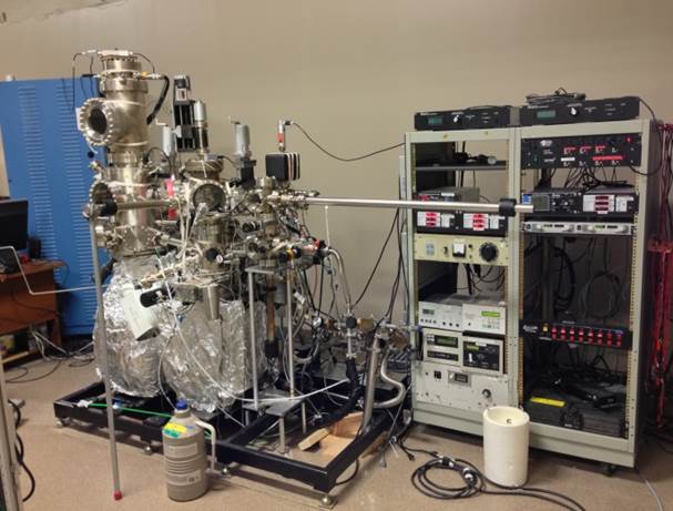
Mr. Randall then introduced scanning tunneling microscopy, or STM, whose development won the Nobel Prize in physics in 1986. The working principle of STM is a tip that is biased at a certain voltage and moved across a surface, detecting surface features by the changing magnitudes of tunneling currents. The tip can also modify the surface.
Mr. Randall then demonstrated the technology of Zyvex Labs -- a STM-tip-based fabrication technology applied to a planar, initially passivated surface of covalent-bonded silicon atoms in their diamond-lattice crystal structure, the well-known silicon(100) surface. On this surface, silicon atoms form dimer rows with sub-nm width and pitch. Targeting specific hydrogen bonds on the surface, the STM tip breaks these and creates dangling bonds. New materials can then be introduced to bond to these newly-open locations. This technique is called “Hydrogen depassivation lithography.†By going down a single line of dimers, a sub-nanometer-precision line can be created, which is impossible with other lithography techniques. If the STM tip is biased at higher voltages, in the “field-emission modeâ€, the removal proceeds faster but less precisely. Combining these methods, we can rapidly define large features and precisely create smaller features. Using a “pixel†size of 2x2 atoms, Zyvex has demonstrated as small as 3 nm by 3 nm perfect squares, geometric designs, cartoons, logos and similar features.
Mr. Randall pointed out that this is a digital process: The bond is either dangling or closed, the address grid is laterally quantized and can be read as well as written to. There is some tolerance to the tip position thanks to the digital nature of the resist.
Mr. Randall then listed applications. He pointed out that new semiconductor device designs such as the single-atom transistor are made possible by precise dopant placement in semiconductor layers. Selective dopant deposition to enable this technology has been demonstrated with phosphorus in silicon.
Applications include building atomically precise metrology standards, MEMS oscillators, and very precise molds to stamp on membranes. With such templates, you can create patterns for fabricating higher density magnetic storage media, which are otherwise approaching density limits. Hard mask deposition and pattern transfer to create material layers to act as hard masks are also possible. This enables the creation of more precise tools to use in conventional semiconductor processing.
Mr. Randall emphasized that the strategy is exploiting this high resolution technology for these applications, while aiming for absolute precision and reproducibility, to manufacture much larger items with no error accumulation for stronger, more reliable macro-scale products.
Finally, Mr. Randall pointed out that with Moore's law, integrated circuit size has stayed approximately the same while the complexity increased. With absolute precision, you can get exponential growth in size as well as complexity in semiconductor technologies. He left the audience with the thought: What will happen to life expectancy, transportation and communication with this new area of scaling enabled?
Mr. Ingersoll then solicited questions from the audience. On correcting defects in this process, Mr. Randall stated that while you can remove unremoved atoms with a second pass, the technique as yet cannot replace mistakenly removed atoms. Discussing defects, he pointed out that some spurious depassivation away from the target could be observed, but for most applications these one-offs do not matter. To a question about the stability of patterns created with this technique, Mr. Randall responded that at room temperature the patterns are stable.
To the question of whether there is any particular thing Mr. Randall would like to create, Mr. Randall responded by listing biomedical possibilities, such as designing molecular interactions and designed enzymes. He also expressed a wish to work on nanorobots to help with further nanomanufacturing, and smart scanners and small controllers for nano-positioning.
Afterwards Mr. Ingersoll thanked the speaker, made the usual housekeeping announcements, and invited guests to apply for membership. At 10:02 pm, President John Ingersoll adjourned the 2,322nd meeting to the social hour.
Attendance: 82
The weather: Mostly Cloudy
The temperature: 17°C
Respectfully submitted,
Zeynep Dilli
Member-at-Large