Chip Scan: 3D X-Ray Imaging of CMOS Integrated Circuits
Can you trust the electronics you use?
Anthony F.J. Levi
Professor and Chair of Electrical and Computer Engineering -- Electrophysics
Department of Electrical and Computer Engineering
University of Southern California
Sponsored by PSW Science Member Adarsh Deepak
About the Lecture
New developments in state-of-the-art ptychographic x-ray laminography microscopy can be used to verify that the most sophisticated integrated circuits and other critical electronic components have been manufactured according to customer design. In principle, billions of CMOS transistors and their metal interconnects can be imaged in three dimensions using this chip-scan technique. The method, which makes use of coherent x-rays, allows reinspection of areas of interest at different levels of resolution. Not only is this of potential interest for non-destructive reverse engineering of integrated circuits, metrology, identification of manufacturing defects and counterfeit products, but it also enables a path to a certified trust service to ensure integrated circuits are manufactured as specified.
Selected Reading & Media References
(1) The x-ray technology that reveals chip designs, A. F. J. Levi and G. Aeppli, IEEE Spectrum, April 30, 2022, https://spectrum.ieee.org/chip-x-ray
(2) Three-dimensional imaging of integrated circuits with macro- to nanoscale zoom, M. Holler, et al., Nature Electronics 2, 464-470 (2019).
About the Speaker
Anthony F. J. Levi (Tony) is Professor and Chair of Electrical and Computer Engineering – Electrophysics in the Department of Electrical and Computer Engineering
at the University of Southern California, where he has been on the faculty for almost 30 years. Before joining the USC faculty he was with AT&T Bell Laboratories for ten years.
Tony invented hot electron spectroscopy, discovered ballistic electron transport in heterostructure bipolar transistors, demonstrated room temperature operation of unipolar transistors with ballistic electron transport, created the first microdisk laser, and carried out work in parallel fiber optic interconnect components in computer and switching systems.
His current research interests include device physics at the classical-quantum boundary, system engineering and integration, high-performance electronics and optimization in system design, RF photonics, very small lasers and modeling their behavior, optimal design of small electronic and photonic systems, and coherent control of transient dynamics.
Tony is an author on numerous technical publications and five texts: Applied Quantum Mechanics; Essential Classical Mechanics for Device Physics; Essential Semiconductor Laser Device Physics; and Essential Electron Transport for Device Physics. He also is the coeditor of the book Optimal Device Design and of several chapters in other technical books. And he is an inventor in 17 US patents.
Tony earned his BSc at the University of Sussex and his PhD in Physics at the University of Cambridge.
Minutes
On November 18, 2022, from the Powell Auditorium of the Cosmos Club in Washington, D.C. streaming online via Zoom and the PSW Science YouTube channel, President Larry Millstein called the 2,467th meeting of the Society to order. He announced the order of business and welcomed new members. The minutes of the previous meeting were then read and approved.
President Millstein then introduced the speaker for the evening, Anthony F.J. Levi, Professor of Electrical and Computer Engineering at the University of Southern California. His lecture was titled, “Chip Scan: 3D X-Ray Imaging of CMOS Integrated Circuits, Can You Trust the Electronics You Use?”
Sophisticated integrated circuits have become critical technology in everyday lives, with handheld computing technologies being ubiquitous. Because integrated circuits are manufactured across the globe, it is feasible that bad actors could manufacture circuits designed to spy on an unsuspecting public. Continuing the modern technological age therefore requires public trust in their devices.
The speaker then described the importance of increasingly thing glass fibers to integrated circuit technology. During the course of his career, the speaker said those fiber diameters shrunk from 2 microns to 5 nanometers, increasing circuit density and making them billions of times more efficient. He predicts that around 2030, the current exponential increase in innovation will end because the ability shrink fiber width will hit a limit at around 0.001 microns.
The speaker then said that for several years, United States circuit manufacturing has lagged in transistor density relative to manufacturers close with China. He said for that reason, it is reasonable for people to question the trustworthiness of their everyday electronics because there is so much opportunity for malfeasance.
The challenge for evaluating circuit integrity is examining them without destroying them. The conventional approach for looking inside a chip is a destructive delayering process, with no room for error and no ability to perform more than once.
Levi’s team has developed non-destructive chip inspection using coherent x-ray 3D imaging. He described his efforts to assemble the right team to use the technique to achieve useful resolution.
The traditional way to conduct x-ray imaging is to focus a coherent x-ray beam that diffracts from metal layers and produces an intensity pattern that is picked up on a focal plane array of detectors and corresponds to a cross-section of the 3D Fourier transform of a projection trough the sample and corresponds to a cross-section of the 3D Fourier transform of the whole object. Reconstructing the image of the 3D object is finding the field and phase just given the intensity data, requiring many images of a rotating sample.
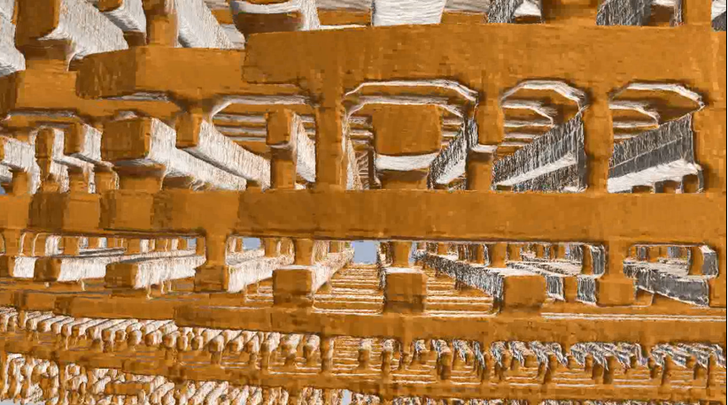
The speaker then described with visuals his team’s current efforts to create three dimensional digital objects that allow users to explore designed circuits. Those renderings can then be “sliced” to reproduce photolithographic masks to compare against imaged data. This method reveals differences between product design and manufacture.
Levi then showed a digital reconstruction of multiple different microprocessors. He compared design models to imaged data and said the data reveals manufacturing fingerprints as to various places of manufacture and engineering quality. He then described the ability to explore and measure circuit materials using x-rays.
The next challenge is to examine objects larger than chips because eventually x-rays cannot penetrate any further. This problem can be addressed with laminography to minimize the unobservable area, and Levi’s team is working on methods to “fill in” the otherwise missing data.
After the question and answer period, President Millstein thanked the speakers, made the usual housekeeping announcements, and invited guests to join the Society. President Millstein then adjourned the meeting.
Temperature in Washington, D.C.: 8 C
Weather: Partly Cloudy
Attendance: 24 in-person and 27 streaming for a total of 51 live viewers and 281 online viewers in the first two weeks of posting.
Respectfully submitted,
James Heelan, Recording Secretary